Introduction
Recently I created a new real-time clock (RTC) module for my slowly growing collection of classic Apple computers.
While the first attempt was working well, the serial timing was always a little tight, when compared to the timings exhibited by the original Apple RTC.
As an example when the original RTC was required to provide data back to the host it’s required to update the data line when the clock is low. In the instances I checked the data line was always updated within 200ns of the falling edge of the clock. Leaving 600ns before the next rising clock edge. My version however would typically update the data line between 40ns and 60ns before the rising clock edge, occasionally missing the deadline altogether and updating the data line just after the rising edge.
A feature of the Microchip ATTiny85 that I considered using was its universal serial interface (USI). While designed to communicate with I2C and SPI devices it’s generic enough to be used for other protocols.
The Apple RTC protocol shares some similarities with I2C. It uses open-collector outputs with resistor pull-ups on its data and clock lines. It’s always clocked by the host and follows a similar address + data scheme for transactions. It lacks however the start / stop sequence and acknowledgment features present in I2C, using its separate enable line to indicate when a transfer is in progress.
A slight snag that stopped me from investigating the USI while originally working on my RTC replacement is that the device would no longer be pin-compatible.
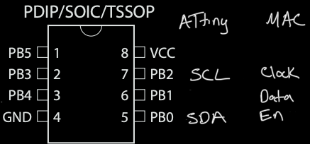
The USI interface in its I2C configuration is exposed on pins PB0 (serial data or SDA) and PB2 (serial clock or SCL). Whereas the Apple RTC uses pin PB0 for its enable signal and places data on PB1. Thereby requiring PB1 and PB0 to be swapped.
Software
Having recently come into possession of a voucher for some PCB prototypes from China I thought it might be time to take the USI module for a spin.
The Microchip ATTiny85 datasheet provides an overview of the operation of the USI peripheral when used for I2C communication:
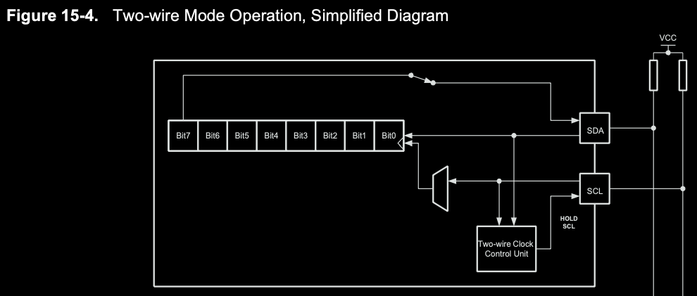
When used for I2C communication the USI hardware at a basic level consists of a data shift register, a clock control unit and a counter.
The data shift register shifts on SCL edges. Sampling the value of the SDA pin on one edge into the least significant bit of the register. While shifting the most significant bit of the register on the other onto the SDA pin (if the pin is configured as an output). For the RTC the shift register will be configured to sample the SDA pin on the rising edge and update it it on the falling edge of the SCL pin when in output mode.
The clock control unit is responsible for detecting I2C start / stop conditions as well as performing the I2C clock stretching feature, providing an I2C device time to process an address and respond appropriately. These features can be safely ignored as the USI module will only drive the SCL line (for example during clock stretching) if the pin is configured as an output.
The counter is the final piece of the puzzle. Its a 4-bit counter, which is incremented on each edge of the SCL line. Therefore when it rolls over we’ve either transmitted or received a complete byte, having counted 16 clock edges.
Both the clock control unit and counter have configurable interrupts for start/stop condition detection and counter roll over respectively.
The idea being to use the pin change interrupt as in my first solution, to monitor the enable line.
When a rising edge is detected on the enable line the USI module will be reset, such that it’s ready to receive the start of the next address / command.
When a falling edge is detected on the enable line the USI counter overflow interrupt flag of the USI will be monitored, waiting for the transfer to complete. Along with the enable line in case the transfer is aborted.
Overall the same general process as before will be followed, replacing the bit bashed serial transfers with calls to the USI module.
For example the previous bit bashed receive routine:
uiBit = 8;
while (0 != uiBit)
{
	/* Sample bit on rising edge, while monitoring enable (except after last bit) */
	while (!mIsClockHigh()) if (mIsEnableHigh()) return;
	uiAddrBase = (uiAddrBase << 1) | mIsDataHigh();
	uiBit--;
	if (0 != uiBit) while (mIsClockHigh()) if (mIsEnableHigh()) return;
}
Becomes:
while (!mIsUSIOIFSet()) if (mIsEnableHigh() || mSerialTimeout()) return;
uiAddrBase = USIBR;
With a similar reduction in code size for the transmit routine.
Having freed up the processor time which was previously occupied by the serial routines, there’s now plenty of time to monitor for serial timeouts. Allowing the RTC to work with a mac which still has a functioning RTC battery if required.
Additionally it reduces the time critical windows in the code down to a single region. That being the case where a read command is provided. The module must look up the data based on the provided address and configure the USI module to transmit the response before the next clock edge. However this was easily achievable with the bit bashed version and remains so with this version.
With the new code in place and enable / data lines haphazardly swapped, the USI module manages to get the serial data stream looking almost identical to that of the original RTC. With the data line changing within 100ns of the falling clock edge when being driven by the RTC.
Hardware
The last step of the journey involves trying to come up with a new “pin compatible” module, which can be dropped in place of an Apple RTC chip. With that in mind I came up with the following:
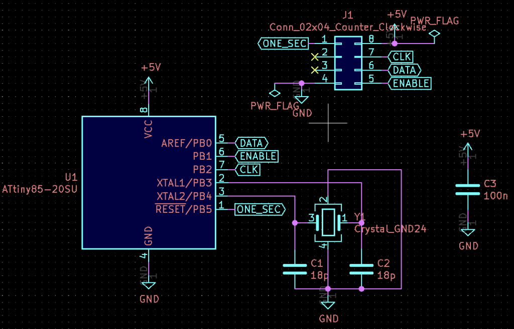
Which becomes the following PCB:


The ATTiny85 in an SOIC SMD package neatly fits between the legs of the original PDIP-8 package. As do its supporting components. While not technically required I took the opportunity to add a crystal oscillator, increasing the timing accuracy, when compared to the internal RC oscillator.
A quick PCB order and dash of hand surface mount assembly and we have something resembling the 3D models above:


The software and hardware designs developed for this project are available on GitHub.
Update: 19th Nov 2024
Following a recent question in the comments, it’s worth nothing that the ATTiny RTC emulator described here can be dropped straight in, in place of Apple’s original RTC chip.
No modifications are required to the logic board. In fact, the battery, diode D1, supplying power to the RTC from the battery and the original crystal Y1 can all be absent.
One slight wrinkle to be aware of. I developed the software for the RTC emulator based on the excellent work of others, building on my previous drop-in replacement software for the ATTiny85. For my battery-less machines, saving the settings and boot options was the most important thing for me. There was some thought put into keeping the RTC running on battery while the machine is off, although this hasn’t been heavily tested. Given the power consumption of the ATTiny85 I don’t suspect it will last a particularly long time when running from an RTC battery.
Having switched from the single chip ATTiny85 solution to this more modular solution would have in hindsight been the perfect time to have addressed the power consumption issue. Unfortunately this wasn’t something I’d considered yet. There may well be a Mk3 module in the future that looks to address this issue.
Leave a Reply